Note: I am reposting this blog post from 2106, as the site hosting it has gone down, but the chip covered is still widely used
GeneralPlus (and SunPlus) microcontrollers contain a mandatory test program in their ROM. It has been long speculated that this program could allow the ROM of any GeneralPlus microcontroller to be dumped. I analyzed the GeneralPlus test program from my Tamagotchi ROM dump, and found it can be used to execute code from RAM, and therefore dump the ROM of the chip.

According to the data sheet (note that the specific model this was dumped from was the GPLB52640A), the test program is from 0xC000 to 0xCBBF, and then its interrupt vectors go up to 0xCBFF. However, when I looked at address 0xC000, it didn’t look like code. Looking at the reset vectors for the user code, I saw the following vectors:
OxFFF2: 0xC2B0
OxFFF4: 0xc104
OxFFF6: 0xC2AF
This is a bit odd, as these pointers to the test program are in the user area of the ROM, but looking at some of the application notes on the GeneralPlus website, it’s not unprecedented for GP to ask users to put specific values in their ROM outside of the test program. Assuming these are in the same order as the regular 6502 reset vectors, these are NMI, RESET and then IRQ. Starting disassembling the code at 0xc104, it looks like a real program

That’s more like it!
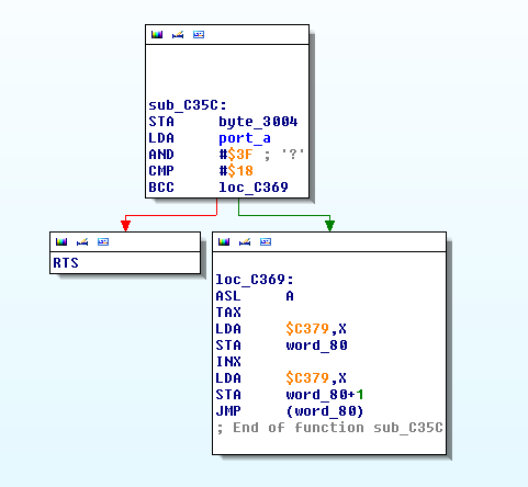
The test program appears to check port 0x3005, and in most cases set a value on port B, and go into a tight loop. But in one situation (I’m assuming this is preliminary tests ‘passing’), it jumps into a subroutine that goes to a different location in a jump table based on the value on port A. This means the chip can run different test cases based on the value on portA when the test program is started. There’s 24 test cases total.

A jump table!
Going through the different locations, here are some notes on the functionality
| Test code | Functionality |
| 0 | Not sure, seems to put device into sleep mode |
| 1 | A whacked out loop that sets and checks a lot of RAM, and then sets a value on port b. Probably a RAM test |
| 2 | More instructions, plus sets to 3004. Perhaps stressing the chip to see if altering that port too much causes arithmetic malfunction |
| 3 | ROM checksum (see details below) |
| 4 | This takes values clocked from port B and sets LCD port values as them. An LCD test. |
| 5 | Takes the value from port B, stores it in 3077, and loops doing this. I wish I knew what port 3077 was for |
| 6 | Reads and writes similar values (0xAA and 0x55) from port A and port B repeatedly. Might be a port stress test |
| 7 | Probably a timer interrupt test |
| 8 | Another LCD test |
| 9 | Stores port B to 3060 and port A to 3062. Not sure what either of these are |
| A | Plays with some ports including 3005. This test is also reachable on startup based on the value of 3005 |
| B | Same test as 9, but 3065 is set to 1, not 2 |
| C | A wakeup test similar to 0 |
| D | Sets LCD values based on port B. Similar to 4 |
| E | Not sure about this one, lots of memory and port manipulation |
| F | Not 100% sure, but I suspect this one is an SPI test |
| 10 | Changes port 300B and 300C, and loc 80 in memory |
| 11 | Another LCD test |
| 12 | Similar to 16 |
| 13 | Same as 3 (the same address is in the jump table twice) |
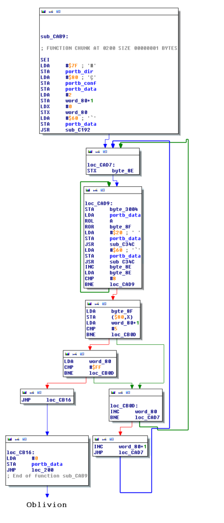
| 14 | Code exec! Input code one bit at a time over p8, p1 and p2 will light up when it’s ready for the next bit. Reading stops at FF once at lead 5 bytes have been read! Code is executed out of RAM at 0x200 |
| 12 | Not sure, there’s an endless loop, so maybe an interrupt test |
| 16 | Just jumps into RAM at 200 (maybe there’s a write to RAM function I missed above) |
| 17 | Sets ports 300B and 300C |
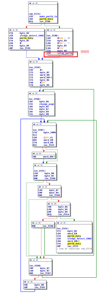
There’s two quite interesting values in here. The first is number 3, which does a checksum of the ROM.

Test Program Test 3
As you can see, there are two options. Either port B is not set, and all pages of the entire ROM is checksummed (note ROM is mapped from 0x4000 to 0xBFFF), or the range to be check-summed is edged in. This might be helpful in dumping ROM (although the smallest range you can checksum is still 255), but it looks like there’s a bug that makes the custom checksums not work. You can see after setting the default addresses, port B is set to be an output, but after setting custom addresses it is not. It’s possible that there’s something I don’t know about port B, and it’s somehow set to be bidirectional already, but my guess is that custom checksums just don’t work. It’s probably not very often that they use a custom range versus the entire ROM.
Test code 14 is also very interesting. It appears to allow you to execute code sent over port B!

This looks like it accepts code over port B.7 one bit at a time, and then sends signals over bits 2 and 4 of port B when it is ready for another bit. It copies the received data to 0x0200 and stops once it reaches the address 0x5FF.
So this could be used to execute code on and dump code from any GeneralPlus microcontroller! The only requirements are that the test pin and ports A and B are available.
The test program is available here if anyone wants to take a look at it.
I’ve also started a list of know ports for the GPLB52640A, I would be very grateful to anyone who contributes


12 responses to The GeneralPlus Test Program